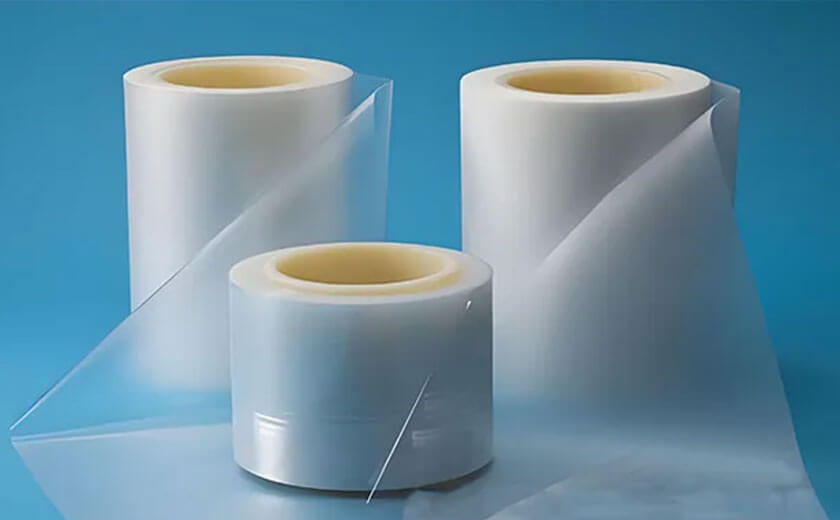
Ethylene Tetrafluoroethylene (ETFE) is a fluoropolymer plastic film that has found specialized, high-value applications within the semiconductor industry, particularly in advanced packaging processes. Its unique combination of properties makes it a material of choice for specific, demanding steps in the fabrication of modern integrated circuits (ICs).
Key Material Properties of ETFE
The utility of ETFE in semiconductor packaging stems from its inherent physical, chemical, and electrical characteristics:
- Excellent Chemical Resistance: ETFE is highly inert and resistant to a wide range of aggressive chemicals used in semiconductor fabs, including strong acids, bases, and solvents. This prevents the film from degrading during cleaning, etching, or plating processes.
- High Thermal Stability: ETFE can withstand continuous operating temperatures typically up to 150°C – 180°C, with short-term peaks even higher. This makes it suitable for high-temperature processing steps without losing its structural integrity.
- Outstanding Dielectric Properties: It possesses a very low dielectric constant (Dk ~2.6) and dissipation factor, which is crucial for minimizing signal loss, crosstalk, and parasitic capacitance in high-frequency applications. This is increasingly important for devices like 5G components and high-performance computing (HPC) chips.
- High Purity and Low Outgassing: ETFE is a very clean material with minimal leachable ions and low outgassing under heat and vacuum. This prevents contamination of sensitive semiconductor surfaces, which is a critical requirement for yield management.
- Mechanical Strength and Durability: It offers high tensile strength, excellent tear resistance, and good abrasion resistance compared to other fluoropolymers like PTFE (Teflon®). This mechanical robustness allows it to withstand the handling stresses of automated manufacturing.
- Low Surface Energy and Non-Stick Properties: Its surface is naturally non-adhesive, which is a double-edged sword. While it prevents materials from sticking, this property is essential for specific release applications.
Primary Applications in Semiconductor Packaging
ETFE film is primarily employed in two critical advanced packaging processes:
1.Temporary Bonding-Debonding for Thin-Wafer Handling:
As wafers are thinned down to sub-100μm levels for 3D integration and to enable more chips per wafer, they become extremely fragile and cannot support their own weight. In the temporary bonding process, the device wafer is bonded to a rigid, temporary carrier wafer using a sacrificial adhesive layer. A layer of ETFE film can be used either as a:
- Release Layer: Placed between the adhesive and the device wafer, its non-stick properties allow for a clean and controlled mechanical debonding (slide-off) once processing on the backside of the thin wafer is complete.
- Bonding Layer: In some film-assisted molding systems, ETFE itself can act as the bonding interface.
This process enables essential backside operations like through-silicon via (TSV) reveal, backside metallization (RDL), and solder bumping.
2.Photoimageable Encapsulant Films:
This is a rapidly growing application. ETFE can be formulated into a photoimageable film. In Fan-Out Wafer-Level Packaging (FOWLP), this film is laminated over a reconstituted wafer containing chips and molding compound. It is then:
- Photoimaged: Using standard lithography tools (exposure through a mask and development), precise openings can be created in the ETFE-based film to expose the underlying chip pads.
- Cured: The film is then fully cured to become a permanent, robust dielectric layer.
This layer acts as the first layer of insulation and environmental protection, over which redistribution layers (RDL) are built to fan out the electrical connections.
Advantages and Limitations
1.Advantages
- Process Simplification: Replaces liquid-based spin-on dielectrics in some applications, offering better uniformity and eliminating solvent-related issues.
- Superior Electrical Performance: Its low Dk is beneficial for high-speed digital and RF devices.
- Reliability: Provides a robust, chemically resistant, and hermetic barrier that enhances the long-term reliability of the packaged device.
- High Throughput: Lamination of dry film is a rapid and scalable process suitable for high-volume manufacturing.
2.Limitations
- Cost: ETFE is significantly more expensive than standard epoxy molding compounds or polyimide films.
- Processing Complexity: Requires specialized equipment for lamination, precise exposure, and development.
- Adhesion: Its low surface energy can pose challenges for achieving strong adhesion to other materials, often requiring surface activation treatments (e.g., plasma) prior to further processing.
Conclusion
ETFE film is a high-performance material enabling key innovations in semiconductor advanced packaging, particularly in the domains of 3D integration and Fan-Out Wafer-Level Packaging. Its role in temporary bonding ensures the manufacturability of ultra-thin wafers, while its use as a photoimageable dielectric provides a critical, high-performance layer for signal redistribution and device protection. While its cost limits its use to high-value applications where its electrical, thermal, and chemical properties are essential, ETFE remains a vital enabler for the continued miniaturization and performance enhancement of modern electronics.
If you have any questions or needs regarding our ETFE Film, please feel free to contact us. Our contact information is as follows:
Phone: +86 15956561251
Email: ruby@mochi.org.cn
Looking forward to working with you to create a bright future!